|
Sr. No.
|
Equipment Name
|
Make & Model and Year of Installation
|
Specification/Attachments
|
Sample Requirement:
|
Application |
About Equipment
|
Photo |
|
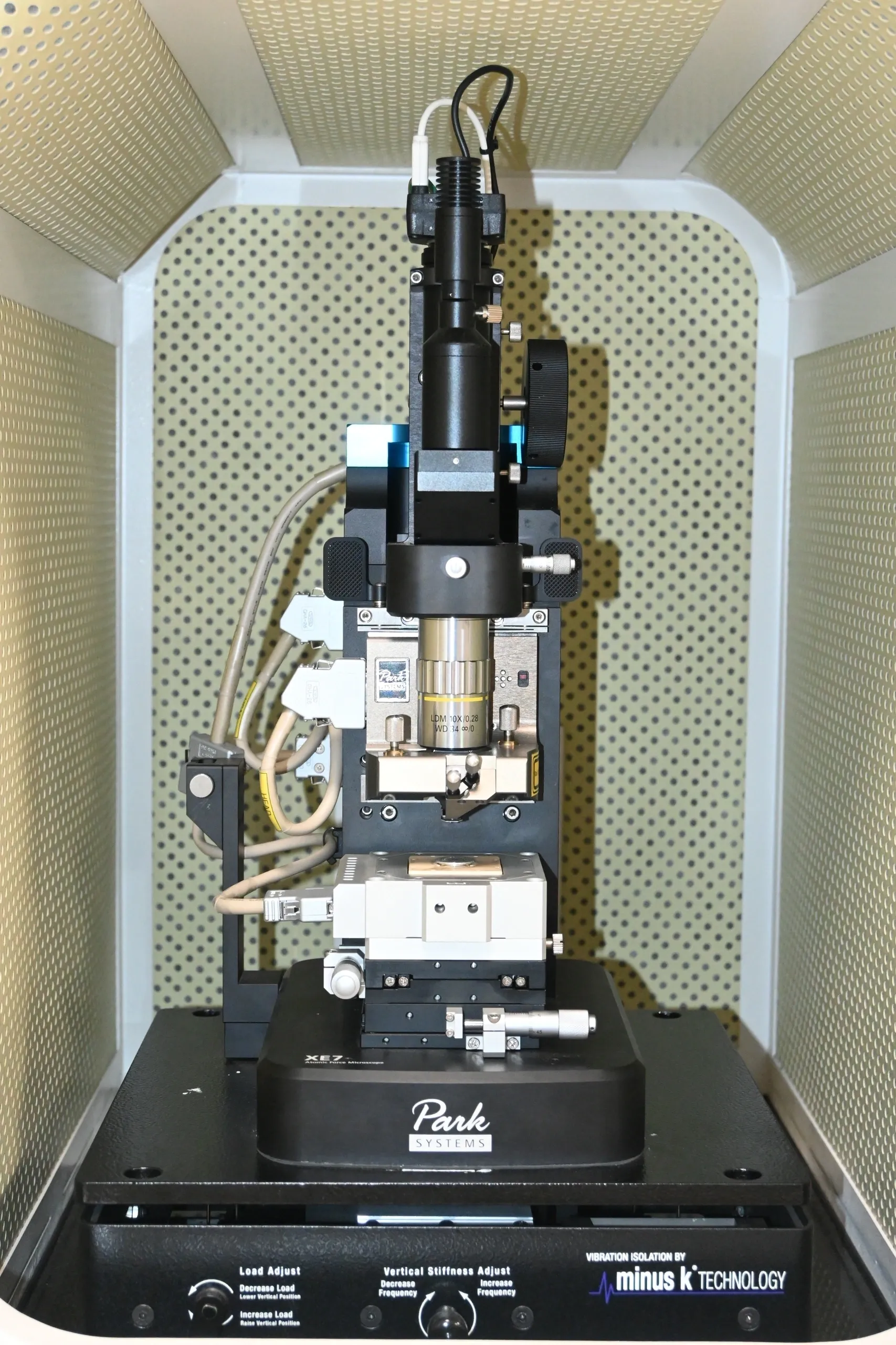
1.
|
Atomic Force Microscopy
|
Park systems, Suwon, Korea,XE7,2014
|
- Software: XEI
- STM
- Normal topography
- SKPFM
- PEM
- Electrochemistry cell
|
Solid (Surface should be plane), Thin film
Thin films are also accepted
|
- Sample morphology
- Height Profile
- Surface roughness
- Work Function
|
Atomic force microscopy (AFM) is a type of scanning probe microscopy (SPM), with demonstrated resolution on the order of fractions of a nanometre, more than 1000 times better than the optical diffraction limit. The information is gathered by "feeling" or "touching" the surface with a mechanical probe. Piezoelectric elements that facilitate tiny but accurate and precise movements on (electronic) command enable precise scanning. Despite the name, the Atomic Force Microscope does not use the nuclear force. It gives you ready access to the largest number of measurement modes in material sciences, stress and texture measurement.
|
 |
|
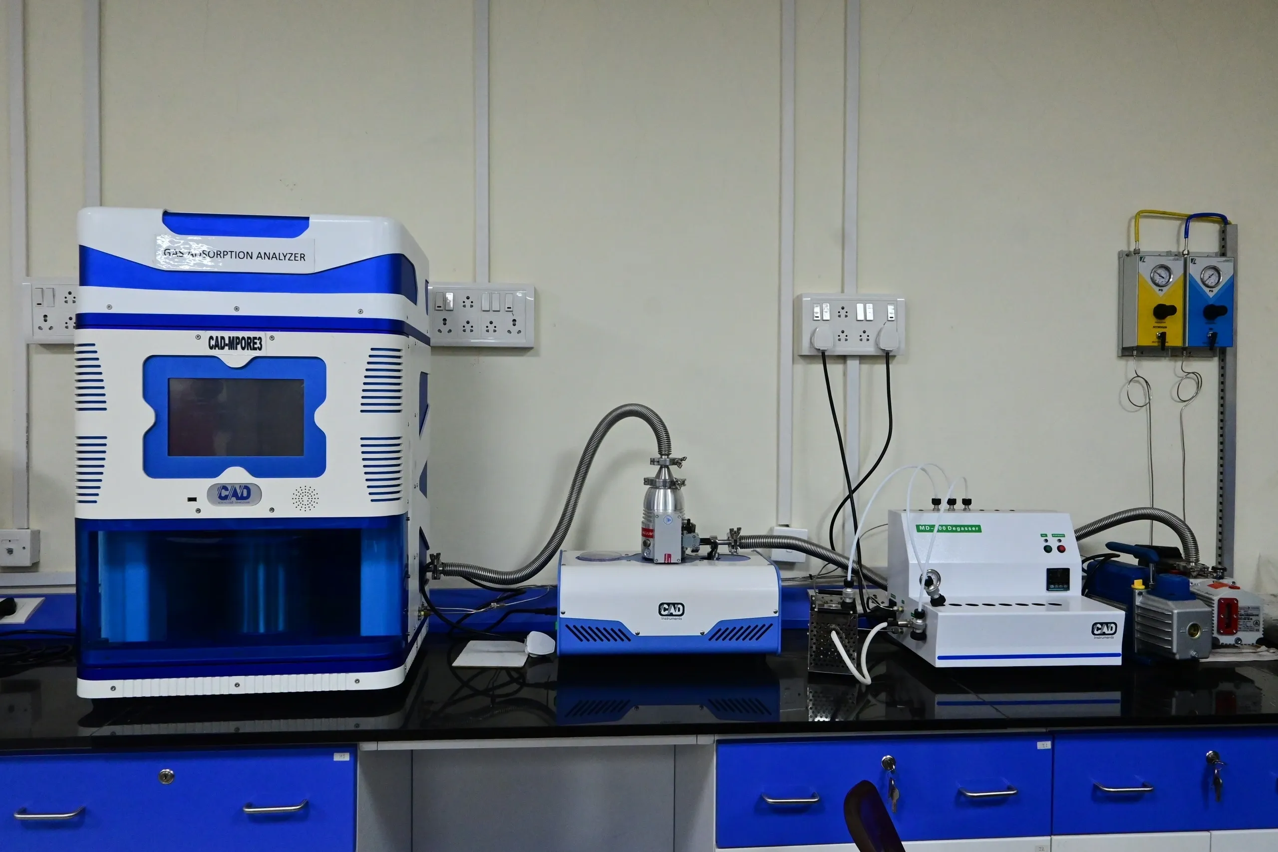
2.
|
BET Surface Area Analyser
BET Requsition form
|
Make: CAD instruments France
Model: CAD-M Pore3
Year of Installation: 2019
|
Software: Stencil wizard
|
Powder (should have weight more than 100mg)
|
- Porosity of material
- Surface area
- Pore diameter
- Pore volume
- t-Plot window
- MP method
- HK Method
- Langmuir plotting window
- αs Plot window
|
Measuring Surface area, Distribution of pores, and pore volume have numerous applications in the study of catalysis, active carbon, pharmaceutical materials, paints, dyes, and polymer materials. BET is the most prominent method to determine accurate pore size and porous area of the material, based on adsorption of specific molecular species in the gas state on their surfaces. BET surface area analyzer used for Checking porosity of polymeric materials, thermal insulators as well as electrical insulators. The surface area of pharmaceutical powders and porous materials can be determined using a BET surface area Analyser. The pharmaceutical industry uses this information when designing drugs, as drugs with a smaller surface area will be metabolized more quickly.
|
 |
|
3.
|
Box Coating Unit
|
Make: HINDHIVAC Vacuum
Model: BC-300
Year of Installation: 2016
|
E-Beam: chromium deposition
Thermal: Gold, Copper etc.
Thickness range: Few micrometre
|
Uniform substrate
|
- |
- The Box Coating Unit is capable of producing clean ultimate vacuum up to 10-6m.bar.
- Coating of various Materials (few nm to thick film)
- Protective coating against solar radiation Interference Filters
- Reflection & Anti-reflection layers
- Anti-corrosive layers
- Semi-conductor layers
|
 |
|
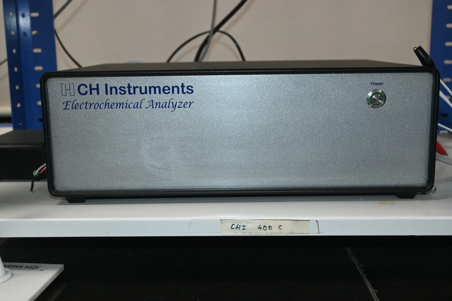
4.
|
CHI-400c electrochemical workstation (QCM)
CHI400 c Requsition form
|
Make: CH instruments
Model: CHI400c
Year of Installation: 2019
|
Software: CHI400c
|
Powder, liquid solution, conducting electrodes modified with the materials, Buffer solutions.
|
- CV
- Quartz Crystal Microbalance (QCM Measurements)
|
The quartz crystal microbalance (QCM) is a variant of acoustic wave microsensors capable of ultrasensitive mass measurements. Under favourable conditions, a typical QCM can measure a mass change of 0.1-1 ng/cm2. QCM oscillates in a mechanically resonant shear mode under the influence of a high-frequency AC electric field applied across the thickness of the crystal. Figure 1b below shows an edge view of a QCM crystal undergoing oscillatory shear distortion. The central portions of the top and bottom of the crystal are coated with a typically disk-shaped thin metal film (e.g., gold). The mass sensitivity of the QCM originates from the dependence of the oscillation frequency on the total mass of the metal-coated crystal, including any adlayers of deposited materials.
|
 |
|
5.
|
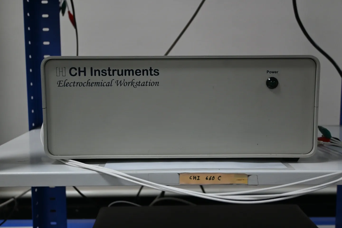
CHI-660c electrochemical workstation
CHI660c Requsition form
|
Make: CH instruments, United state
Model: CHI660c
Year of Installation: 2008
|
Software: CHI660c
|
Powder, liquid solution, conducting electrodes modified with the materials, Buffer solutions,
|
- Potentiostatic study
- Galvanostatic study
- CV
- EIS
- Electrochemical Sensing (CV, DPV, ASV, Amperomettric Detection (I-T curve) etc)
- Electrochemical Synthesis
|
The Model 600C series is designed for general purpose electrochemical measurements. The system contains a fast digital function generator, high-speed data acquisition circuitry, potentiostatic, and a galvanostatic (available only in select models). The potential control range is ±10 V, and the current range is ±250 mA. The instrument is capable of measuring current down to tens of picoamperes. The steady-state current of a 10 mm disk electrode can be readily measured without external adapters. With the CHI200 Picoamp Booster and Faraday Cage (fully automatic and compatible with the CHI600C series), currents down to 1 pA can be measured. These instruments are high-speed. The function generator can update at a 5 MHz rate, and the maximum sampling rate is 1 MHz at 16-bit resolution. The tool provides an extended dynamic range on experimental time scales. For instance, the scan rate in cyclic voltammetry can be up to 500 V/s with a 0.1 mV potential increment or 5000 V/s with a 1 mV potential increment. The potentiostatic/galvanostatic uses a 4-electrode configuration, allowing it to be used for liquid/liquid interface measurements and eliminating the contact resistance of connectors and relays for high current measurements. Multiple data acquisition systems allow an external input signal (such as spectroscopy signals to be recorded simultaneously with electrochemical data). The instrument will also automatically re-zero both potential and current so that periodic re-calibration of the instrument can be avoided. The instrument can be utilized for Electrochemical Sensing, Electrochemical synthesis, CV, EIS, and superconductivity characterizations.
|
 |
|
6.
|
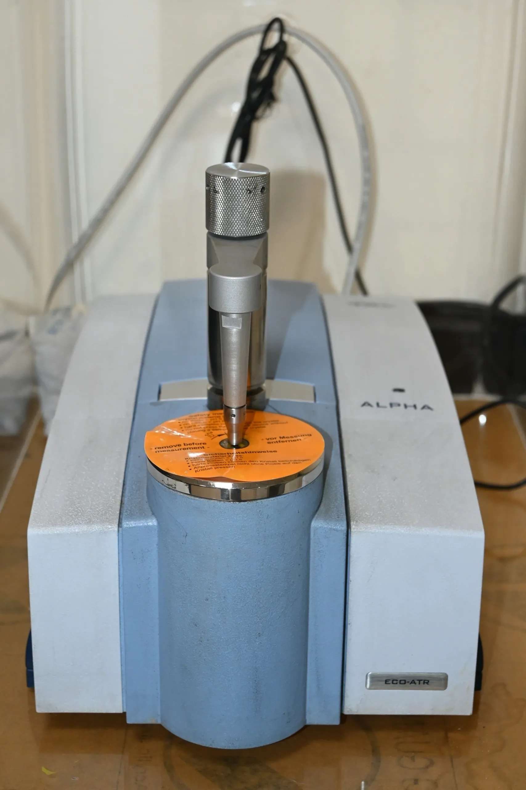
Fourier transform infrared (FTIR) spectroscopy
FTIR Requsition form
|
Make: Bruker
Model: Alpha
Year of Installation: 2013
|
- Wavelength range: 500 cm-1 to 4000 cm-1
- Software: OPUS
Available Window: ZnSe, Ge
|
liquids, solids, powders, semisolids, thin film and pastes.
|
- Chemical Composition and bonding
|
Fourier transform infrared (FTIR) spectroscopy is a specific type of IR spectroscopy. Unlike a dispersive IR spectrometer, where a dispersive element splits the incoming light into its spectral components and where each component is measured individually, one at a time (“scanned”), in FTIR, all frequencies of light are measured simultaneously. The IR spectrum is then obtained via a mathematic conversion called Fourier transformation. Because FTIR spectroscopy measures all frequencies simultaneously, FTIR analysis can be performed much faster compared to a scanning technique. In Fourier transform infrared (FTIR) spectroscopy, all spectral components of the light source are detected together. In order to obtain an FTIR spectrum, the spectral composition of the incoming light is permanently modified. Therefore, the signal detected by the FTIR detector is time dependent. A mathematical operation called Fourier transformation allows us to convert the detector signal from a time domain into the frequency domain (ultimately displayed in wavenumbers, cm-1), which results in the well-known FTIR spectrum. FTIR analysis is also considered resource friendly, as it only requires a small amount of sample, little or no sample preparation, and no consumables. FTIR spectroscopy is also flexible and versatile. It can be applied to a variety of sample types including liquids, solids, powders, semisolids, and pastes, and it delivers quantitative as well as qualitative information.
|
 |
|
7.
|
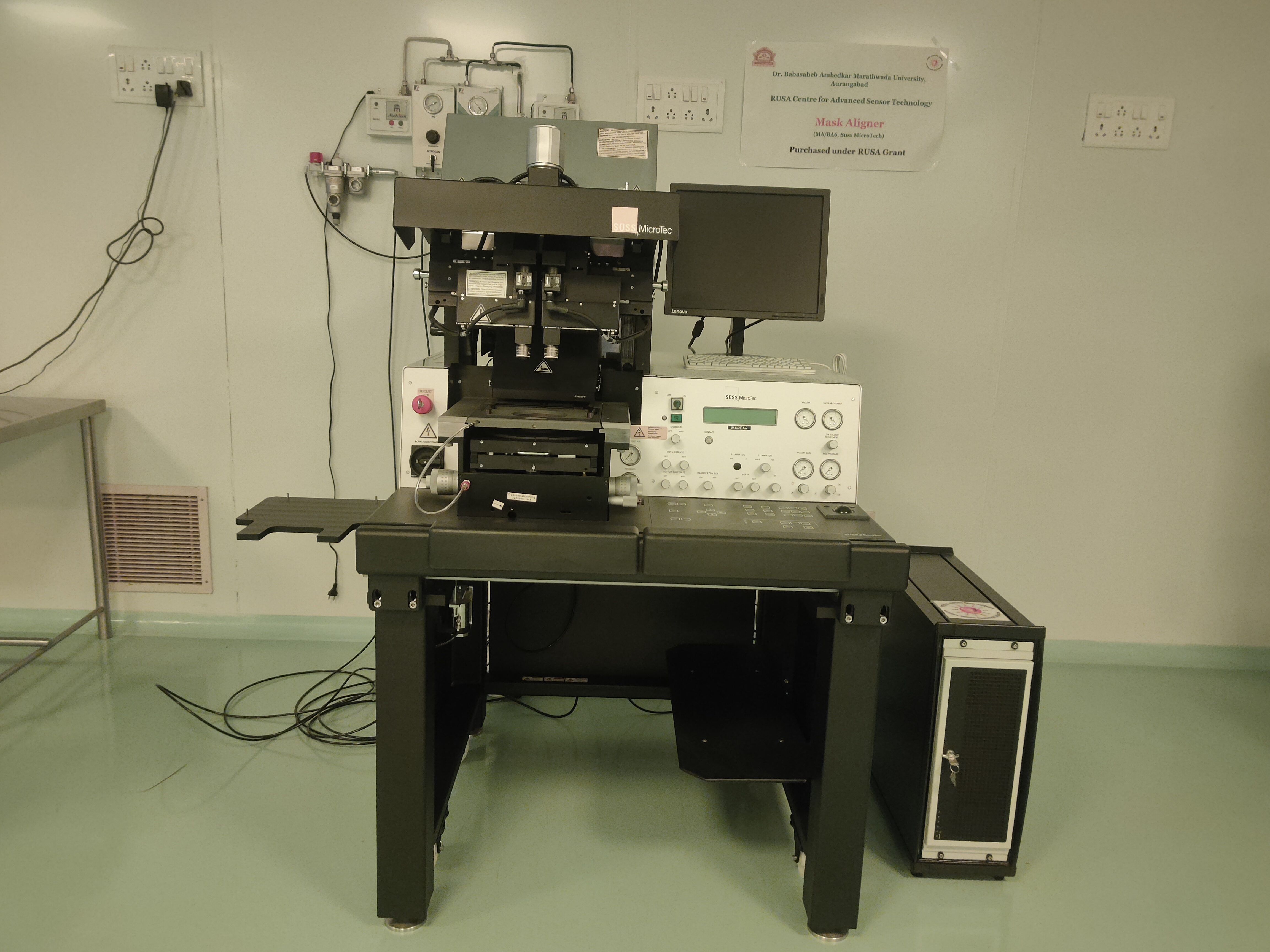
Mask aligner
|
Make: Suss Micro Tec
Model: BA 6
Year of Installation: 2016
|
7.
|
Silicon wafer
|
-- |
- It is a precision machine tool used in process to transfer a pattern onto a wafer or substrate.
- Instead of using conventional time-consuming lithography technique, Mask aligner provides better resolution (more number circuits can be pattern simultaneously).
- Mask aligner enabled photolithography can be used to produce semiconductor devices, such transistors, sensors and medical components.
|
 |
|
8.
|
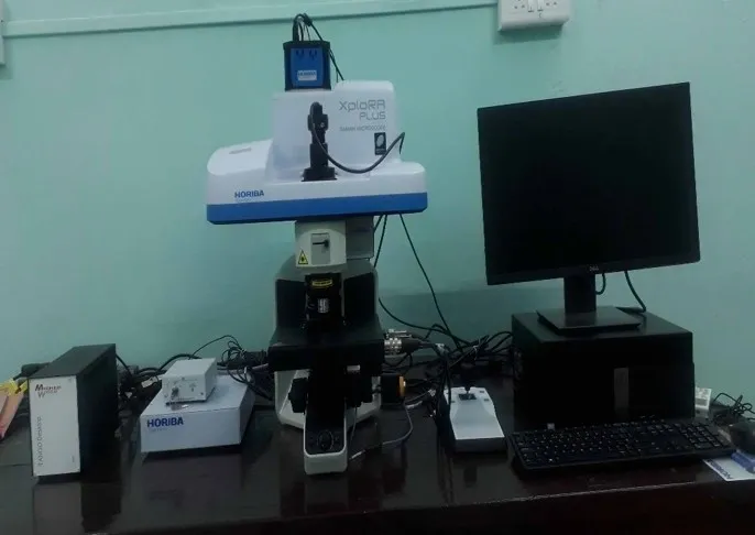
Raman spectroscopy
Raman Requsition form
|
Make: Horiba Scientific France
Model: Xplora Plus
Year of Installation: 2019
|
Excitation Laser Wavelength: 532 nm & 785 nm
Laser Steps: 0.1%, 0.5%, 5%, 10%, 25%, 50% and 100%
Objectives: 5X, 10X, 50X and 100X
|
Thin film, powder form and liquid
|
- characterize the chemical composition
- identification of food fraud and food adulteration
- Identification of minerals.
- Analysis of Compound concentration
- To check whether material is crystalline or not
- Material composition and distribution using Raman mapping.
- Polymer identification
- Photoluminescence spectra measurement
- Contaminant identification
- Surface deformation studies
- Elemental mapping
|
Remi
(named after Indian physicist C. V. Raman) is a spectroscopic technique typically used to determine vibrational modes of molecules, although rotational and other low-frequency modes of systems may also be observed. Raman spectroscopy is commonly used in chemistry to provide a structural fingerprint by which molecules can be identified. Raman spectroscopy relies upon inelastic scattering of photons, known as Raman scattering.
|
 |
|
9.
|
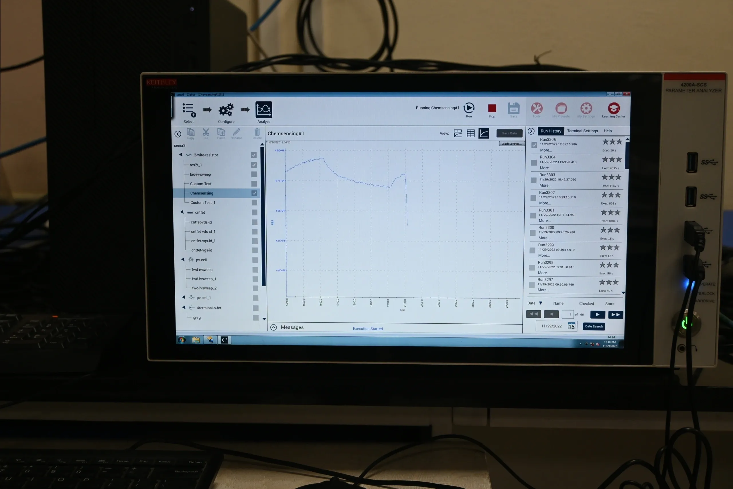
Semiconducting Parameter Analyzer
|
Make: Keithly
Model: 4200
Year of Installation: 2017
|
Software: Clarius
|
Powder drop cast on copper-clad, Conducting sample
|
- IV characteristics
- FET characteristics
- CV characteristics
- Chemiresistive sensing
- Solar cell Application
|
Accelerate research, reliability, and failure analysis studies of semiconductor devices, materials, and process development with the 4200A-SCS. The highest performance parameter analyzer delivers synchronizing current-voltage (I-V), capacitance-voltage (C-V), and ultra-fast pulsed I-V measurements. The 4215-CVU offers low-noise capacitance measurements at frequencies 1 kHz to 10 MHz. With the 4201-SMU and 4211-SMU modules, you can achieve stable low current measurements in a high capacitance system. With four models of source measure unit (SMU) to choose from, the 4200A-SCS can be customized to meet all of your I-V measurement needs. By offering field Installable Units and optional preamplifier modules, Keithley makes sure that you can make the most accurate low current measurements with little to no downtime. In addition, Keithley Care plans provide fast, high-quality services at a fraction of the cost of on-demand service events
|
 |
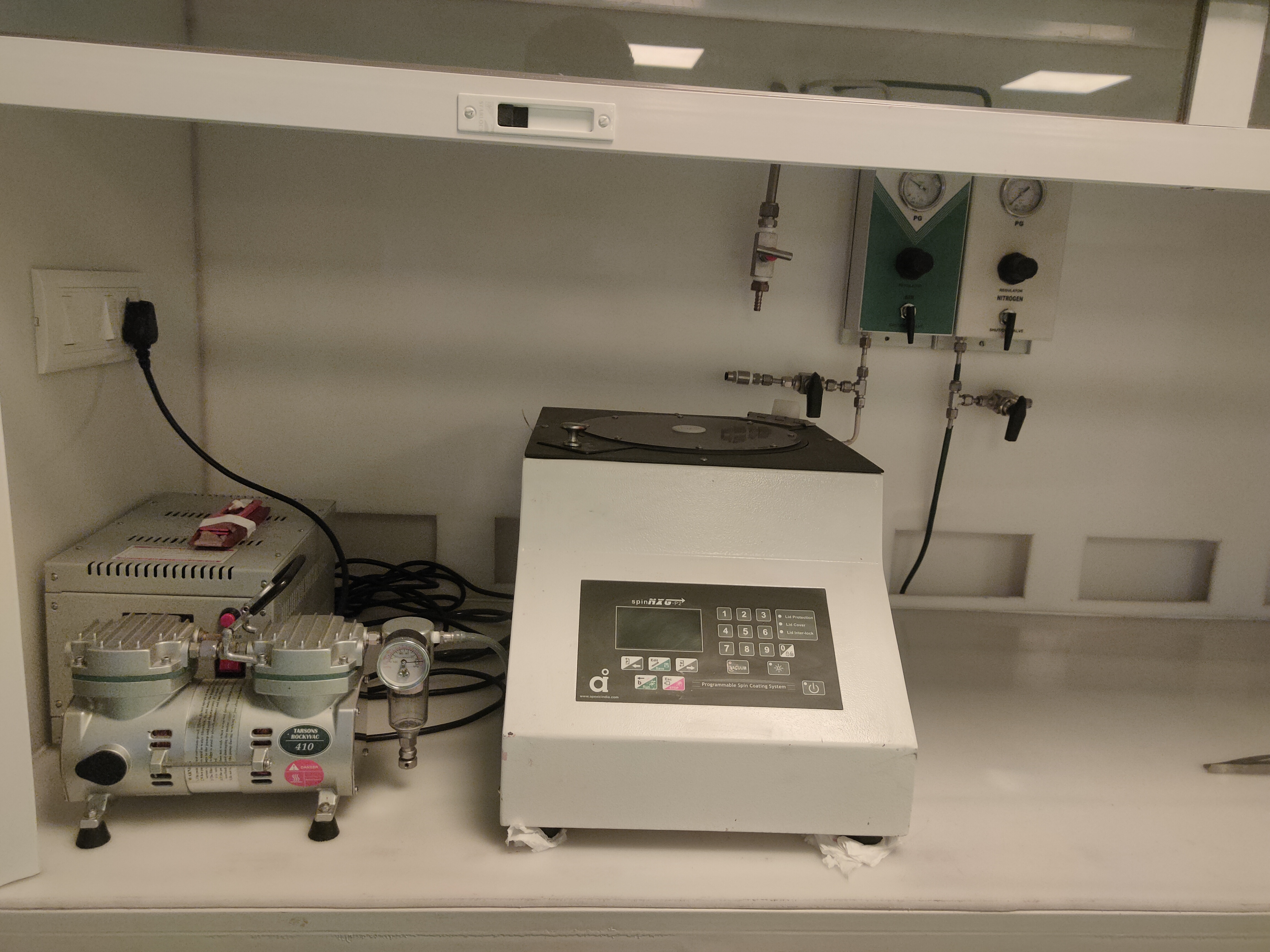
| 10. |
Spin Coater |
REMI; R-24 |
|
Plane circular substrate
|
- Photoresist for defining patterns in microcircuit fabrication.
- Organic light emitting diodes
- Organic field effect transistors.
- Synthetic, Bio and Dielectric/insulating layers for microcircuit fabrication – polymers, SOG, Si, etc.
- Flat screen display coatings. - Antireflection coatings, conductive oxide, etc.
- Pattering and etching, solar cells, Hybrid organic, Inorganic devices.
|
Spin coating is a procedure used to deposit uniform thin films onto flat substrates. Usually, a small amount of coating material in liquid form is applied on the centre of the substrate, which is either spinning at low speed or not spinning at all. The substrate is then rotated at speeds up to 10,000 rpm to spread the coating material by centrifugal force. A machine used for spin coating is called a spin coater, or simply spinner
|
 |
| 11. |
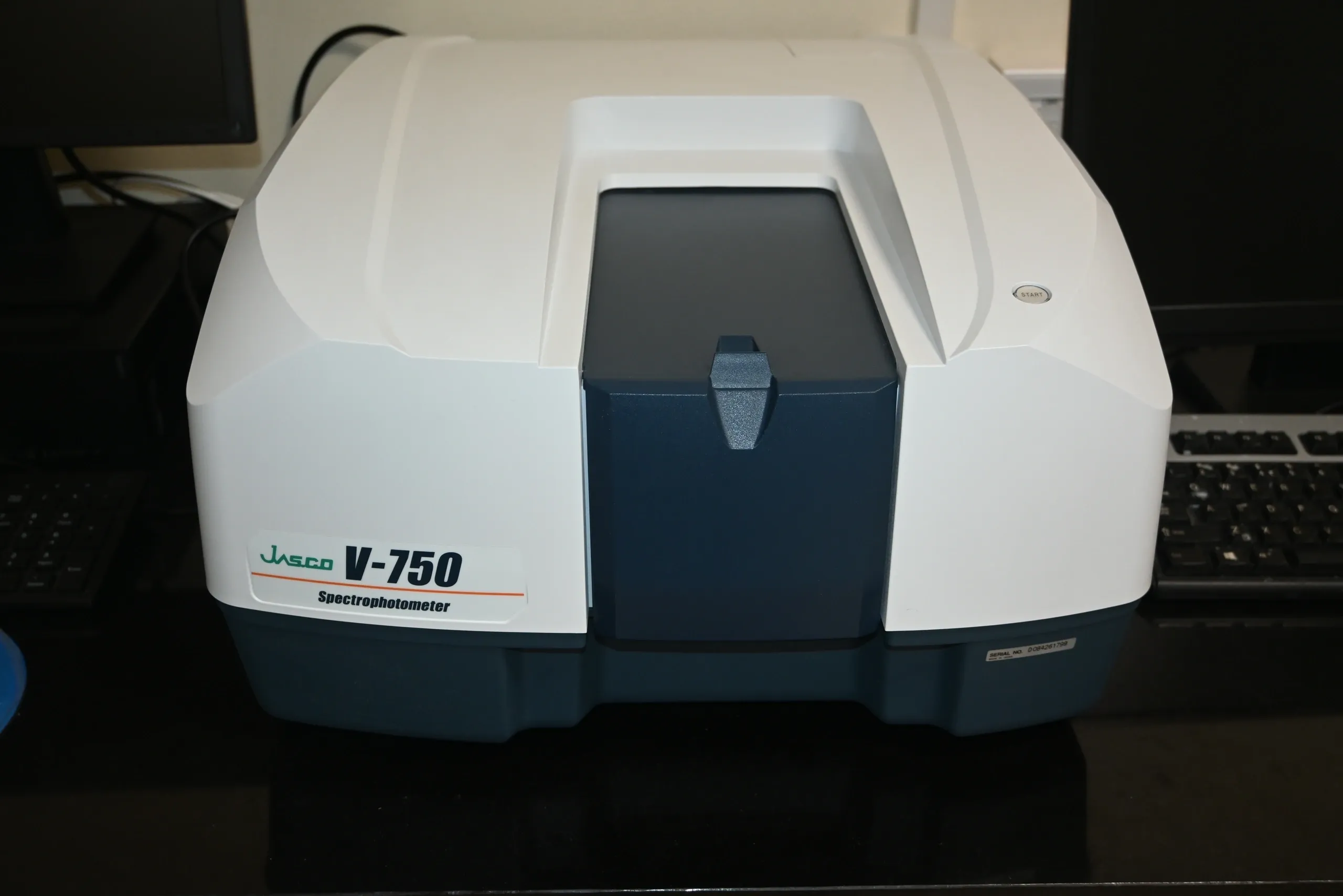
UV- Visible spectroscopy
UV-Vis Requsition form
|
Model: JASCO V-750
Year of Installation: 2019
|
Specification: Wavelength range –200-900 nm
Software: Spectra Manager
|
Powder,
|
- UV/Vis spectroscopy is usually applied to organic molecule
- Measure how much chemical substances absorb the light
- Detection of impurities in compound.
- It can provide valuable information about compounds, and impurities.
- Identify and quantify information about the atoms and molecules in a sample
- drug identity, test purity, drug crystalline structures
- UV Spectrophotometry Identifies Compounds in Pharmaceutical
- information about the levels of active ingredients presents in pharmaceutical compounds, as well as detect any impurities
- Measuring the molecular and metabolic changes that occur
|
Spectroscopy is used as a tool for studying the structures of atoms and proceed molecules This is done by measuring the intensity of light that absorb/transmitted through a sample. |
 |
| 12. |
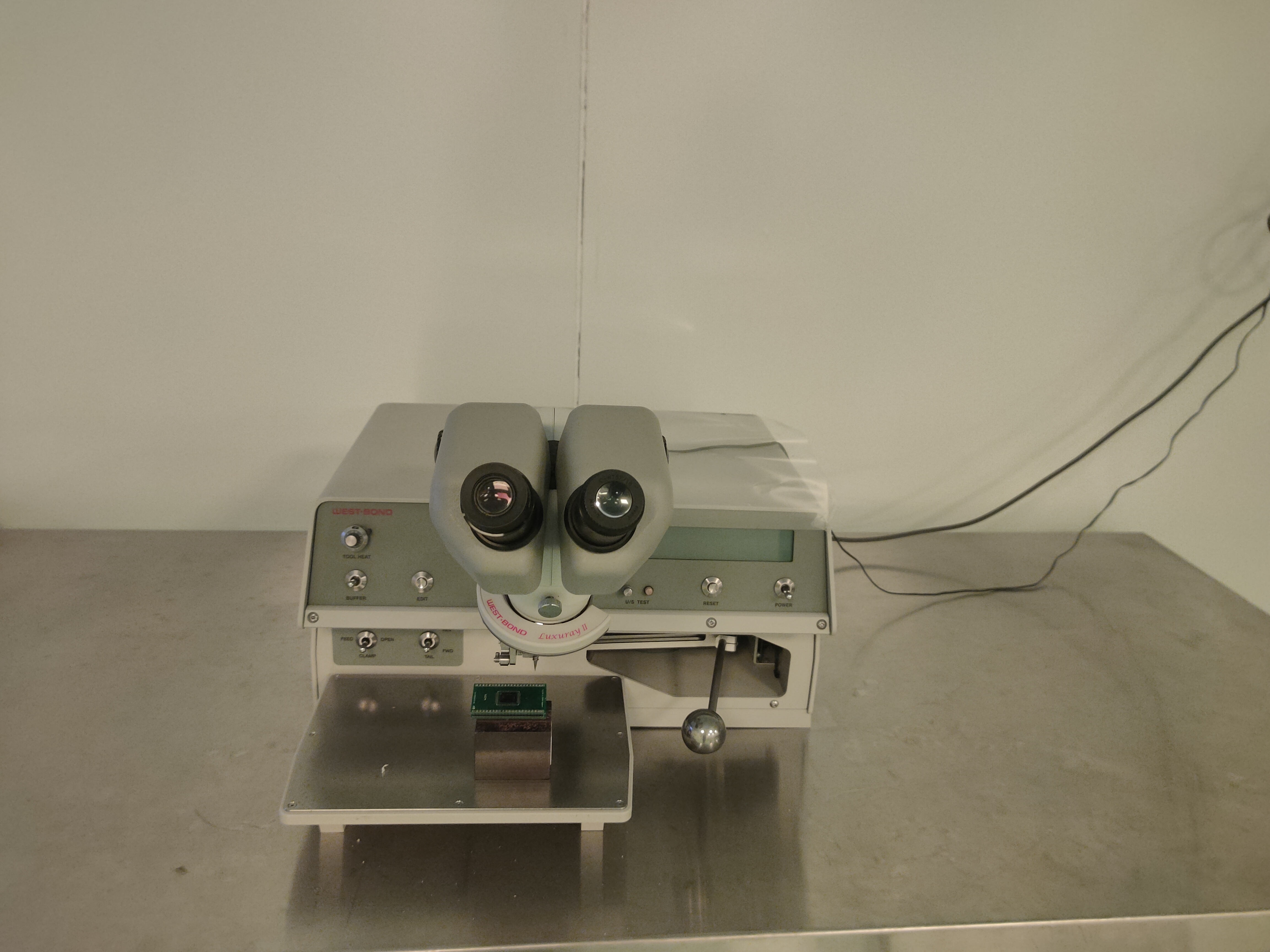
Wire bonder
|
Make: HINDHIVAC Vacuum
Model: BC-300
Year of Installation: 2016
|
|
|
-- |
- Wire bonding is the method of making interconnections between an integrated circuit (IC) or another semiconductor device.
- Gold and Aluminium wires are being used for wire bonding
- Wire diameters start at 15 μm and up to several hundred micrometres for high-powered applications.
|
 |
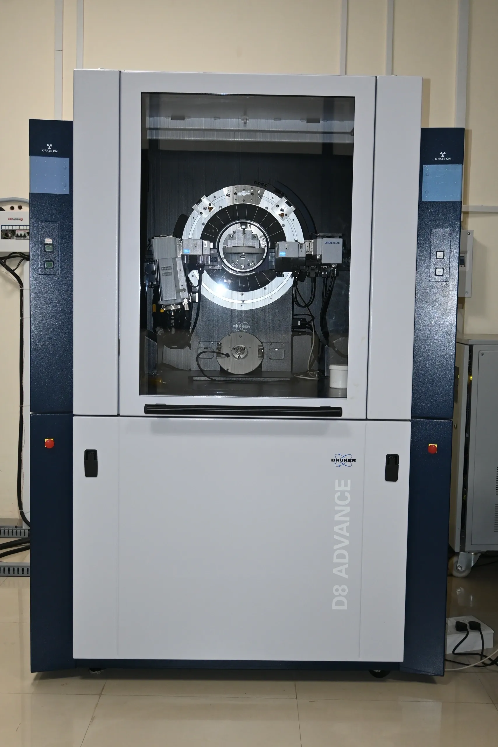
| 13. |
X-ray Diffraction (XRD)
XRD Requsition form
|
Make- Bruker
Model- D8-Advance
Year of Installation- 2016
|
X-Ray Source: 2.2kW Cu anode, 40 kV/40 mA
Detector: LINXEYE XE
Smallest angular step size: 0.0001o
Reproducibility: +/- 0.0001o
Angular range (2Theta): 3o to 130o
|
Amount- 0.5 g (in fine powder form)
Thin films are also accepted
|
- Full width half Maxima (FW)
- Crystallite Size (D)
- Crystallinity
- Interplanar Spacing (d)
- Miller indices (h k l)
- micro strain
- dislocation density
|
X-ray Diffraction (XRD) is a high-tech, non-destructive technique for analyzing a wide range of materials, including fluids, metals, minerals, polymers, catalysts, plastics, pharmaceuticals, thin-film coatings, ceramics, solar cells and semiconductors. Throughout industry and research institutions, XRD has become an indispensable method for materials investigation, characterization and quality control. Example areas of application include qualitative and quantitative phase analysis, crystallography, structure and relaxation determination, texture and residual stress investigations.
The Bruker D8 Advance X-ray diffractometer is designed to easily accommodate all X-ray diffraction applications in material research, powder diffraction and high-resolution diffraction. All new D8 goniometry is equipped with stepper motors with optical encoder to ensure extremely precise angular values. The D8 X-ray Diffractometer can be used for nearly all X-ray diffraction application, such as structure determination, phase, PDF, analysis, stress and texture measurement.
|
 |